
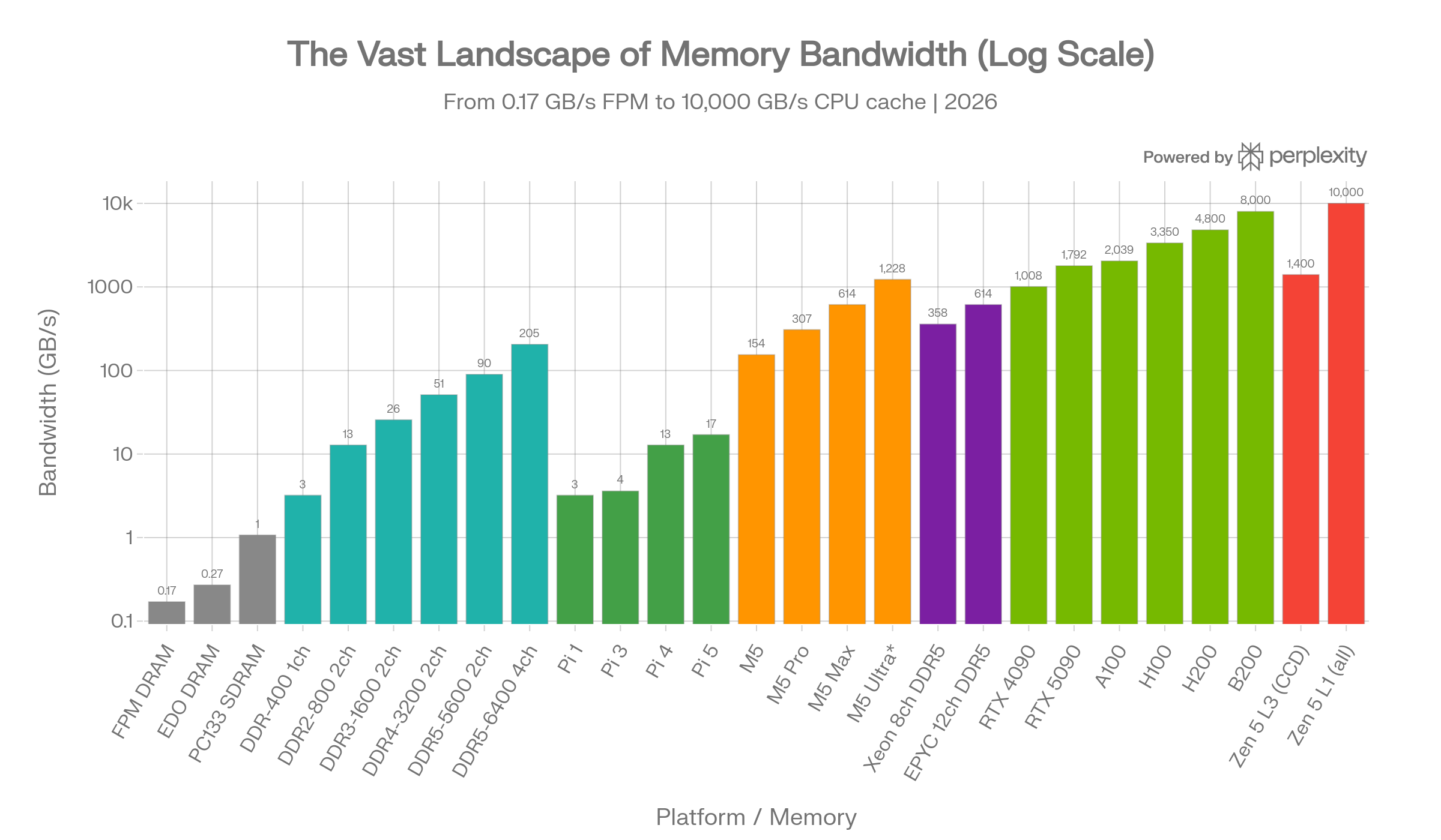
Memory bandwidth spans an almost incomprehensible range - from 0.17 GB/s on legacy FPM DRAM to over 10,000 GB/s inside a modern CPU's L1 cache. This report provides a comprehensive tour through every major tier of the memory hierarchy as of March 2026, covering legacy pre-DDR memory, DDR1-DDR5 in consumer multi-channel configurations, Apple's unified memory architecture across all M1-M5 variants, the humble Raspberry Pi, server-class memory platforms, NVIDIA's AI GPU lineup, HBM's history from AMD Fiji to HBM4, consumer GPU memory, and finally the humbling speed of on-die CPU caches.
Pre-DDR Legacy Memory
Before DDR SDRAM arrived, PC memory evolved through several generations, each roughly doubling the bandwidth of its predecessor.
| Memory Type | Bus Speed | Bus Width | Peak Bandwidth |
|---|---|---|---|
| FPM DRAM | ~22 MHz | 64-bit | ~0.17 GB/s |
| EDO DRAM | ~33 MHz | 64-bit | ~0.27 GB/s |
| PC66 SDRAM | 66 MHz | 64-bit | ~0.53 GB/s |
| PC100 SDRAM | 100 MHz | 64-bit | ~0.80 GB/s |
| PC133 SDRAM | 133 MHz | 64-bit | ~1.07 GB/s |
| RDRAM (dual-ch) | 400 MHz | 2x16-bit | ~3.2 GB/s |
FPM (Fast Page Mode) RAM could cycle at 15-25 MHz in real systems, while EDO DRAM pushed up to 33-50 MHz. SDRAM was the breakthrough that synchronized memory with the system bus, running at 66-133 MHz and nearly doubling EDO's performance. Intel briefly pushed RDRAM (Rambus) for Pentium 4, which achieved higher bandwidth through a narrow but fast serial interface, but its high cost and latency kept it from widespread adoption.1234
DDR1-DDR5: Single, Dual, and Quad Channel
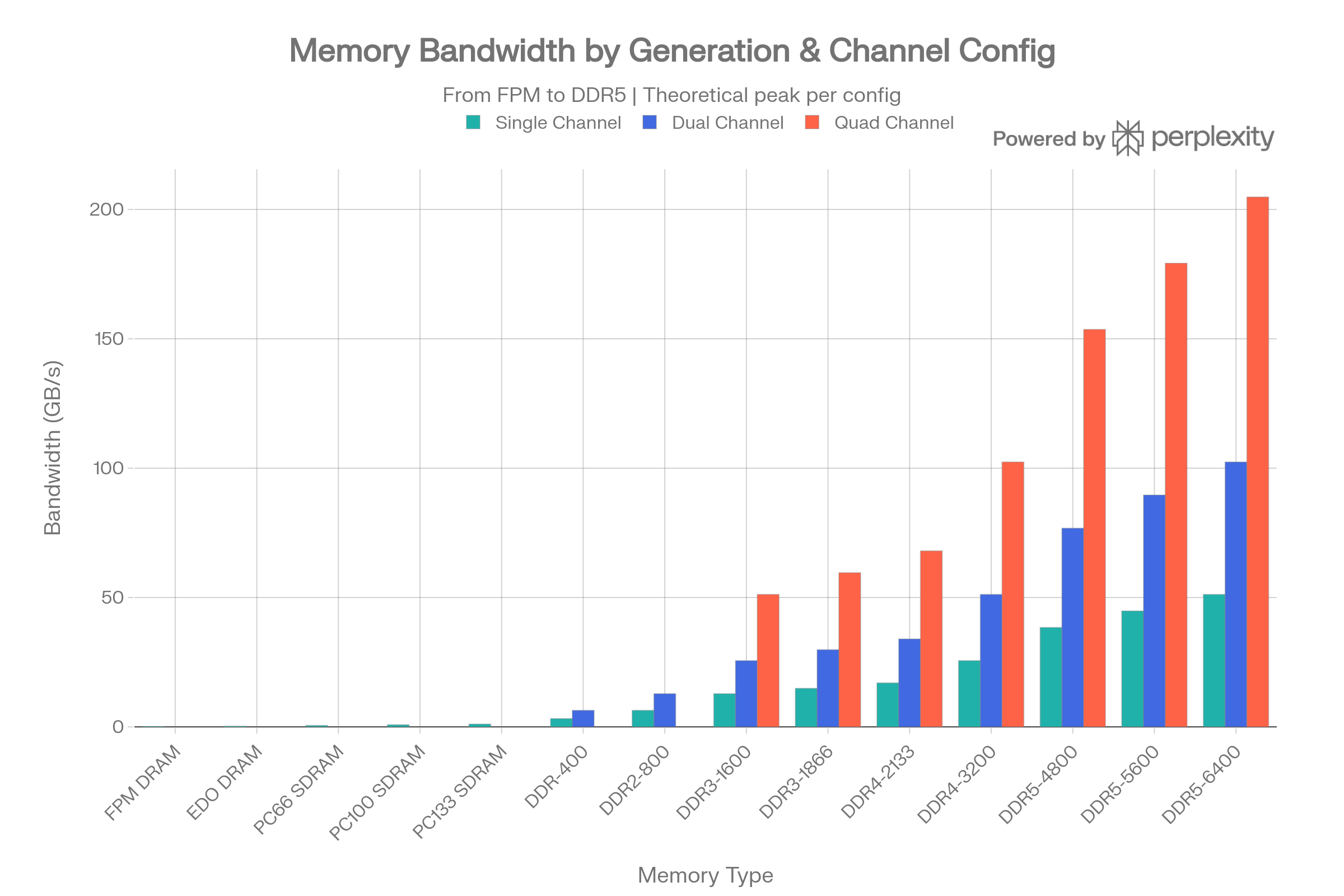
The DDR (Double Data Rate) family has dominated system memory for over two decades. Each generation roughly doubles per-pin data rates. The key insight for workstations is that multi-channel configurations multiply bandwidth linearly.5
Per-Channel Theoretical Bandwidth
| Generation | Common Speed | MT/s | 1-Ch (GB/s) | 2-Ch (GB/s) | 4-Ch (GB/s) |
|---|---|---|---|---|---|
| DDR1 | DDR-400 | 400 | 3.2 | 6.4 | 12.8 |
| DDR2 | DDR2-800 | 800 | 6.4 | 12.8 | 25.6 |
| DDR3 | DDR3-1600 | 1,600 | 12.8 | 25.6 | 51.2 |
| DDR3 | DDR3-1866 | 1,866 | 14.9 | 29.8 | 59.6 |
| DDR4 | DDR4-2133 | 2,133 | 17.0 | 34.0 | 68.0 |
| DDR4 | DDR4-3200 | 3,200 | 25.6 | 51.2 | 102.4 |
| DDR5 | DDR5-4800 | 4,800 | 38.4 | 76.8 | 153.6 |
| DDR5 | DDR5-5600 | 5,600 | 44.8 | 89.6 | 179.2 |
| DDR5 | DDR5-6400 | 6,400 | 51.2 | 102.4 | 204.8 |
All values are theoretical peaks calculated as: Bus Width (64 bits = 8 bytes) x Transfer Rate (MT/s) x Number of Channels. A mainstream desktop with dual-channel DDR5-5600 achieves up to ~89.6 GB/s - the theoretical max for Intel's i9-14900K. Workstation platforms using quad-channel DDR5 (e.g., Intel HEDT, Threadripper) can push past 200 GB/s. Real-world tests on DDR5 quad-channel showed approximately 62.7 GB/s read bandwidth vs. 31.6 GB/s in dual channel - nearly a perfect 2x scaling.678
Apple Silicon: Why Unified Memory is King (M1-M5)
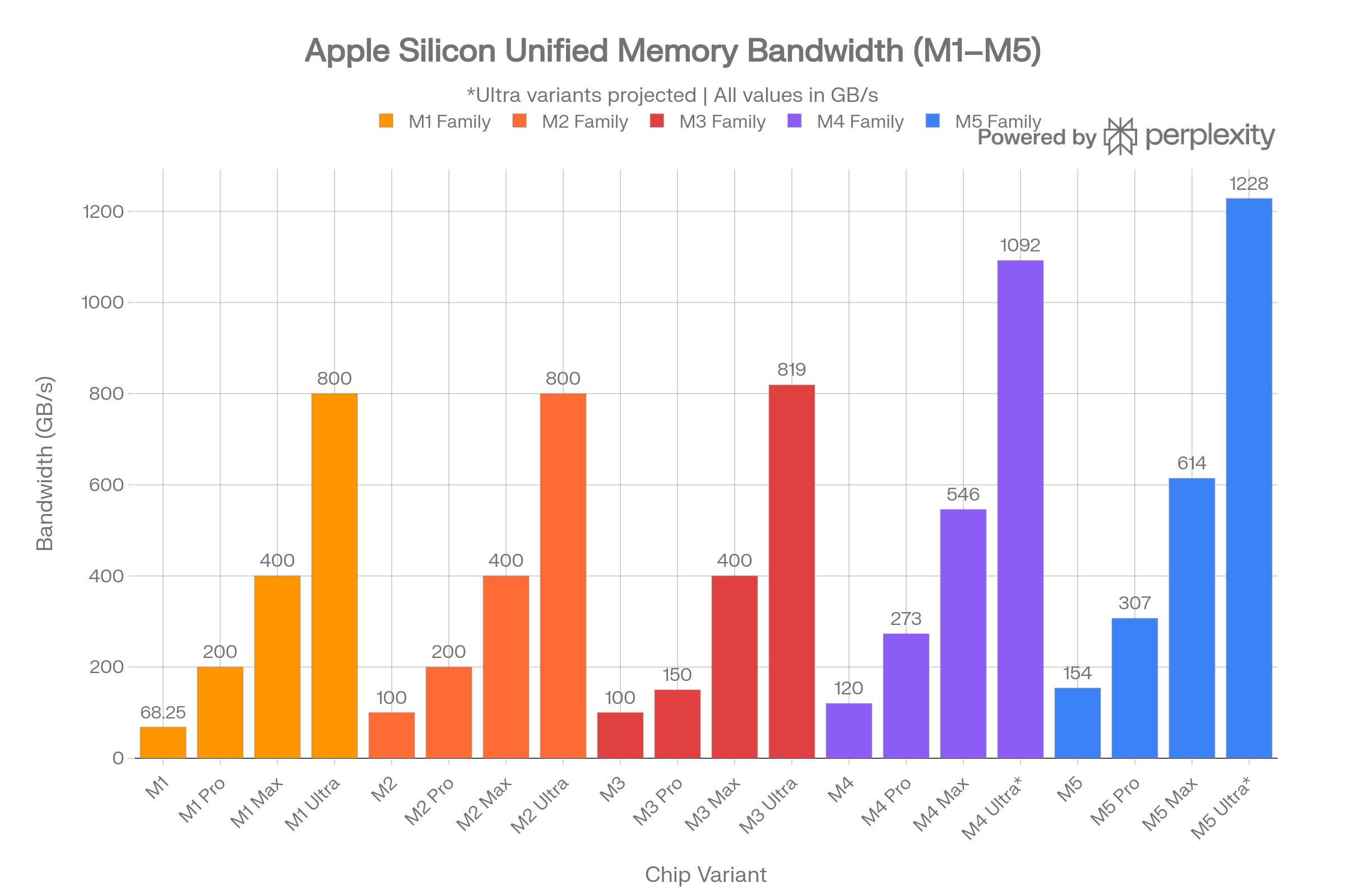
Apple's unified memory architecture is the single best argument for why APU-style designs are the future. By packaging LPDDR memory directly onto the SoC, Apple eliminates the bus bottleneck between CPU, GPU, and Neural Engine - every component shares the same high-bandwidth memory pool with zero-copy overhead.
Complete Apple Silicon Memory Bandwidth Table
| Chip | Year | Max RAM | Bandwidth (GB/s) |
|---|---|---|---|
| M1 | 2020 | 16 GB | 68.25 |
| M1 Pro | 2021 | 32 GB | 200 |
| M1 Max | 2021 | 64 GB | 400 |
| M1 Ultra | 2022 | 128 GB | 800 |
| M2 | 2022 | 24 GB | 100 |
| M2 Pro | 2023 | 32 GB | 200 |
| M2 Max | 2023 | 96 GB | 400 |
| M2 Ultra | 2023 | 192 GB | 800 |
| M3 | 2023 | 24 GB | 100 |
| M3 Pro | 2023 | 36 GB | 150 |
| M3 Max (40-core GPU) | 2023 | 128 GB | 400 |
| M3 Ultra | 2024 | 192 GB | 819 |
| M4 | 2024 | 32 GB | 120 |
| M4 Pro | 2024 | 64 GB | 273 |
| M4 Max (40-core GPU) | 2024 | 128 GB | 546 |
| M4 Ultra (projected) | - | 256 GB | ~1,092 |
| M5 | 2025 | 32 GB | 154 |
| M5 Pro | 2026 | 64 GB | 307 |
| M5 Max (40-core GPU) | 2026 | 128 GB | 614 |
| M5 Ultra (projected) | - | 256 GB | ~1,228 |
The base M5 uses LPDDR5X at 9600 MT/s, delivering 153.6 GB/s - a nearly 30% increase over M4. The M5 Pro doubles this to 307 GB/s, while the top M5 Max hits 614 GB/s. The projected M5 Ultra (two M5 Max dies via UltraFusion) would deliver approximately 1,228 GB/s - exceeding many server-class memory configurations.9101112131415
Why This Matters for AI/ML
The M4 Max's 546 GB/s already provides "4x the bandwidth of the latest AI PC chip". For local LLM inference, memory bandwidth is the primary bottleneck. An M5 Max with 128 GB at 614 GB/s can serve a ~70B parameter model at usable token rates - something no discrete-GPU consumer system with DDR5 main memory can match, because a discrete GPU must copy data across PCIe. Unified memory eliminates this copy entirely.1617
Raspberry Pi 1-5: The Humble End of the Spectrum
The Raspberry Pi family illustrates how single-board computers have evolved from barely usable memory bandwidth to respectable performance.
| Model | Year | RAM Type | Bus Width | Speed | Theoretical BW |
|---|---|---|---|---|---|
| Pi 1 | 2012 | 512 MB LPDDR2 | 32-bit | ~400 MHz | ~3.2 GB/s |
| Pi 2 | 2015 | 1 GB LPDDR2 | 32-bit | ~400 MHz | ~3.2 GB/s |
| Pi 3 | 2016 | 1 GB LPDDR2 | 32-bit | ~450 MHz | ~3.6 GB/s |
| Pi 4 | 2019 | 1-8 GB LPDDR4-3200 | 32-bit | 3200 MT/s | ~12.8 GB/s |
| Pi 5 | 2023 | 1-16 GB LPDDR4X-4267 | 32-bit | 4267 MT/s | ~17 GB/s |
The Pi 1 used the BCM2835 SoC with a single ARM11 core and LPDDR2 clocked at 400 MHz. Real-world stream bandwidth was under 0.2 GB/s due to the weak memory controller. The Pi 4 jumped to LPDDR4-3200, and the Pi 5's BCM2712 documentation confirms "up to 17 GB/s of memory bandwidth" from its LPDDR4X-4267 interface. That's a 5x increase from Pi 1 to Pi 5, but the 32-bit bus width remains the fundamental bottleneck - the Pi 5's 17 GB/s is still less than a single DDR4-2133 DIMM on a desktop.718192021
Server Memory Architectures
Server platforms achieve massive aggregate bandwidth by scaling memory channels far beyond consumer platforms.
| Platform | Channels/Socket | Memory Type | Speed | BW/Socket (GB/s) |
|---|---|---|---|---|
| Intel Xeon Ice Lake (3rd Gen) | 8 | DDR4-3200 | 3200 MT/s | ~204.8 |
| Intel Xeon Sapphire Rapids (4th Gen) | 8 | DDR5-4800 | 4800 MT/s | ~307.2 |
| Intel Xeon Emerald Rapids (5th Gen) | 8 | DDR5-5600 | 5600 MT/s | ~358.4 |
| AMD EPYC Genoa (9004) | 12 | DDR5-4800 | 4800 MT/s | ~460.8 |
| AMD EPYC Turin (9005) | 12 | DDR5-6400 | 6400 MT/s | ~614.4 |
| Intel Xeon Max (w/ HBM) | 8+HBM | DDR5 + HBM2e | - | ~1,638 (HBM) |
AMD's EPYC 9005 series (Turin) with 12 DDR5 channels at 6400 MT/s delivers 614.4 GB/s per socket - a 30%+ improvement over the prior 9004 generation at DDR5-4800. In dual-socket configurations, aggregate bandwidth exceeds 1.2 TB/s. Intel's Sapphire Rapids with 8 channels at DDR5-4800 delivers 307.2 GB/s per socket, while the Xeon Max series adds on-package HBM2e for up to 1,638 GB/s of HBM bandwidth per socket. AMD EPYC supports up to 12 memory channels per socket vs. Intel Xeon's 8, giving AMD a structural bandwidth advantage.222324252627
NVIDIA AI Accelerator GPUs
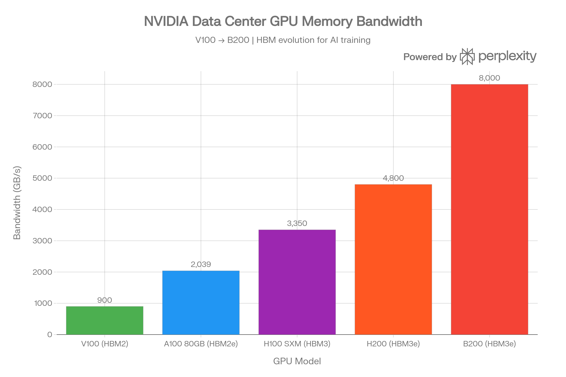
The GPUs powering AI training and inference at companies like OpenAI, Google, Meta, and xAI represent the bleeding edge of memory bandwidth, all enabled by HBM (High Bandwidth Memory).
| GPU | Year | Architecture | Memory | Capacity | Bandwidth |
|---|---|---|---|---|---|
| V100 | 2017 | Volta | HBM2 | 16/32 GB | ~900 GB/s |
| A100 SXM | 2020 | Ampere | HBM2e | 80 GB | 2,039 GB/s |
| H100 SXM | 2022 | Hopper | HBM3 | 80 GB | 3,350 GB/s |
| H200 SXM | 2023 | Hopper | HBM3e | 141 GB | 4,800 GB/s |
| B200 | 2024 | Blackwell | HBM3e | 192 GB | 8,000 GB/s |
| AMD MI300X | 2023 | CDNA 3 | HBM3 | 192 GB | 5,300 GB/s |
The progression is staggering: from the V100's ~900 GB/s to the B200's 8,000 GB/s in just seven years - a nearly 9x increase. The H200 provides 43% more bandwidth than the H100 (4.8 vs. 3.35 TB/s) by switching from HBM3 to HBM3e. The B200 doubles the H100's capacity and achieves 2.4x its bandwidth. AMD's MI300X competes with 192 GB of HBM3 at 5.3 TB/s.2829303132
Consumer/Prosumer NVIDIA GPUs
| GPU | Memory | Capacity | Bandwidth |
|---|---|---|---|
| RTX 3090 | GDDR6X | 24 GB | 936 GB/s |
| RTX 4080 | GDDR6X | 16 GB | 717 GB/s |
| RTX 4090 | GDDR6X | 24 GB | 1,008 GB/s |
| RTX 5090 | GDDR7 | 32 GB | 1,792 GB/s |
The RTX 5090's jump to GDDR7 with a 512-bit bus delivers 1,792 GB/s - a 77% increase over the RTX 4090. For local AI workloads, the RTX 3090's 24 GB with 936 GB/s remains popular in the r/LocalLLaMA community due to its VRAM capacity advantage over the 4080.33343536
HBM: From AMD's Fiji to HBM4
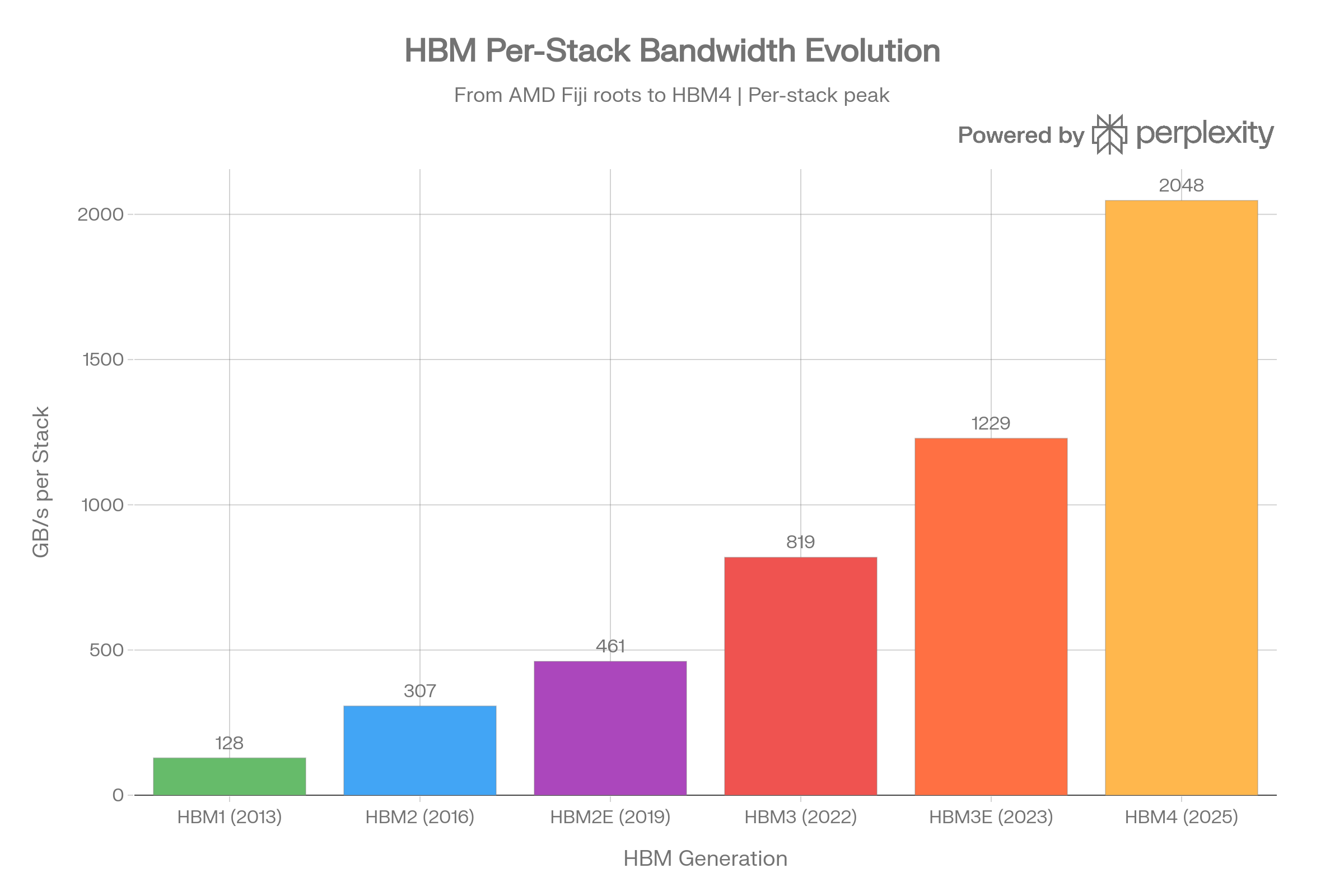
High Bandwidth Memory was born from a collaboration between AMD, Samsung, and SK Hynix, with JEDEC standardizing HBM1 in October 2013. The first production HBM chip came from SK Hynix in 2013, and AMD's Fiji GPU (Radeon R9 Fury X, 2015) was the first device to ship with HBM.37
HBM Generation Specifications (Per Stack)
| Generation | Year | Data Rate/Pin | Interface | Max Capacity | Max Bandwidth |
|---|---|---|---|---|---|
| HBM1 | 2013 | 1.0 Gb/s | 8x128-bit | 4 GB | 128 GB/s |
| HBM2 | 2016 | 2.4 Gb/s | 8x128-bit | 8 GB | 307 GB/s |
| HBM2E | 2019 | 3.6 Gb/s | 8x128-bit | 24 GB | 461 GB/s |
| HBM3 | 2022 | 6.4 Gb/s | 16x64-bit | 24 GB | 819 GB/s |
| HBM3E | 2023 | 9.8 Gb/s | 16x64-bit | 48 GB | 1,229 GB/s |
| HBM4 | 2025 | 8.0 Gb/s | 32x64-bit | 64 GB | 2,048 GB/s |
HBM achieves its extraordinary bandwidth through a massively wide 1024-bit interface (per stack) combined with 3D die stacking via through-silicon vias (TSVs). AMD's Fiji used HBM1 with ~512 GB/s across 4 stacks. The Vega GPU moved to HBM2, with the Vega 56 achieving 409.6 GB/s across 2 stacks. Samsung's HBM2E "Flashbolt" pushed a single package to 410 GB/s with 3.2 Gbps per pin. HBM3 introduced 16 pseudo-channels and pushed data rates to 6.4 Gb/s, hitting 819 GB/s per stack. The upcoming HBM4 doubles the interface to 2048 bits and supports up to 2 TB/s per stack.383937
The Humbling Finale: CPU Cache Speeds
After reviewing everything from 0.17 GB/s FPM DRAM to 8 TB/s B200 HBM bandwidth, CPU caches put it all in perspective. The fastest memory in any system isn't external at all - it's the on-die SRAM caches sitting millimeters from the execution units.
AMD Ryzen 9 9950X (Zen 5)
| Cache Level | Size | Per-Core BW | All-Core Aggregate |
|---|---|---|---|
| L1 Data | 48 KB/core (768 KB total) | ~650 GB/s | >10,000 GB/s |
| L2 | 1 MB/core (16 MB total) | ~300+ GB/s | - |
| L3 | 32 MB/CCD (64 MB total) | - | ~1,400 GB/s (per CCD) |
| DRAM (DDR5-6000) | - | - | ~96 GB/s (theoretical) |
With all 16 cores loaded, the Ryzen 9 9950X delivers over 10 TB/s of L1 data cache bandwidth. That's more than the NVIDIA B200's 8 TB/s HBM3e - except it's happening inside a $600 desktop CPU. Zen 5 achieves this with dual 512-bit vector load paths per core, a 50% increase in L1D capacity over Zen 4, and an improved 32-byte-per-cycle L3 interface. Per-CCD L3 bandwidth of ~1.4 TB/s is itself nearly as fast as the Xeon Max's total HBM bandwidth.40
Intel Core i9-14900K (Raptor Lake)
| Cache Level | Size |
|---|---|
| L1 Data (P-core) | 48 KB x 8 cores |
| L1 Data (E-core) | 32 KB x 16 cores |
| L2 (P-core) | 2 MB x 8 cores |
| L2 (E-core cluster) | 4 MB x 4 clusters |
| L3 | 36 MB shared |
| DRAM (DDR5-5600) | 89.6 GB/s max8 |
Intel's Raptor Lake's all-core L1 cache bandwidth falls significantly behind Zen 5's 10 TB/s figure. The hybrid architecture with 16 Gracemont E-cores delivers less cache bandwidth per core, and Intel disabled AVX-512 in consumer parts - removing the 2x512-bit load path that Golden Cove originally supported. The P-cores still pack 2 MB of L2 each with ~12-cycle latency, and the 36 MB shared L3 provides solid hit rates for gaming workloads.404142
The Cache Bandwidth Perspective
Bandwidth Comparison Tool
To truly appreciate the hierarchy:
| Tier | Example | Bandwidth |
|---|---|---|
| Legacy DRAM | FPM DRAM (1995) | 0.17 GB/s |
| Modern Desktop RAM | DDR5-5600 Dual-Ch | 89.6 GB/s |
| Apple M5 Max | Unified LPDDR5X | 614 GB/s |
| Server (EPYC Turin) | 12-ch DDR5-6400 | 614 GB/s |
| AI GPU (B200) | 192 GB HBM3e | 8,000 GB/s |
| CPU L3 Cache (Zen 5) | 32 MB SRAM/CCD | ~1,400 GB/s |
| CPU L1 Cache (Zen 5) | 48 KB SRAM/core | >10,000 GB/s |
The L1 cache is over 58,000x faster than FPM DRAM and roughly 111x faster than the DDR5-5600 dual-channel system memory feeding the same CPU. This is why cache hit rates matter so much - every miss that falls through to main memory encounters a 100x bandwidth penalty and an even worse latency penalty (from ~1 ns L1 to 70+ ns DRAM).40
Why APU Unified Memory Wins
The data tells a clear story about why unified memory architectures are increasingly dominant for AI and creative workloads:
- No copy overhead: Discrete GPUs must shuttle data across PCIe (64 GB/s Gen 5). Apple's unified memory lets CPU, GPU, and Neural Engine all access the same pool at 614 GB/s on M5 Max.10
- Bandwidth density: An M5 Max delivers 614 GB/s in a laptop form factor. Matching that with desktop DDR5 requires a quad-channel workstation platform.
- Capacity advantage: The M5 Max supports 128 GB of memory accessible by the GPU - vs. consumer GPUs that top out at 24-32 GB of VRAM.1133
- Power efficiency: LPDDR5X on-package draws far less power than GDDR or HBM solutions, enabling this bandwidth in a ~30W laptop chip envelope.
The tradeoff is clear: HBM-equipped data center GPUs still dominate in raw bandwidth (8 TB/s on B200), but unified memory designs offer the best bandwidth-per-watt and eliminate the PCIe bottleneck for heterogeneous workloads where CPU and GPU share data constantly.
References
Footnotes
-
Types of RAM: How to Identify and their Specifications - Technibble ↩
-
Guide DDR DDR2 DDR3 DDR4 and DDR5 Bandwidth by Generation - ServeTheHome ↩ ↩2
-
Apple introduces MacBook Pro with all-new M5 Pro and M5 Max ↩ ↩2
-
New MacBook Pro M5 Pro and M5 Max announced - Tom's Guide ↩ ↩2
-
NVIDIA GeForce RTX 3090 vs 4080 Super for AI - BestGPUsForAI ↩
-
HBM2E: The E Stands for Evolutionary - Semiconductor Engineering ↩
-
AMD's Ryzen 9950X: Zen 5 on Desktop - Chips and Cheese ↩ ↩2 ↩3
-
A Preview of Raptor Lake's Improved L2 Caches - Chips and Cheese ↩